- 您现在的位置:买卖IC网 > Sheet目录3881 > PIC18F8585T-I/PT (Microchip Technology)IC PIC MCU FLASH 24KX16 80TQFP
PIC18F6585/8585/6680/8680
DS30491C-page 278
2004 Microchip Technology Inc.
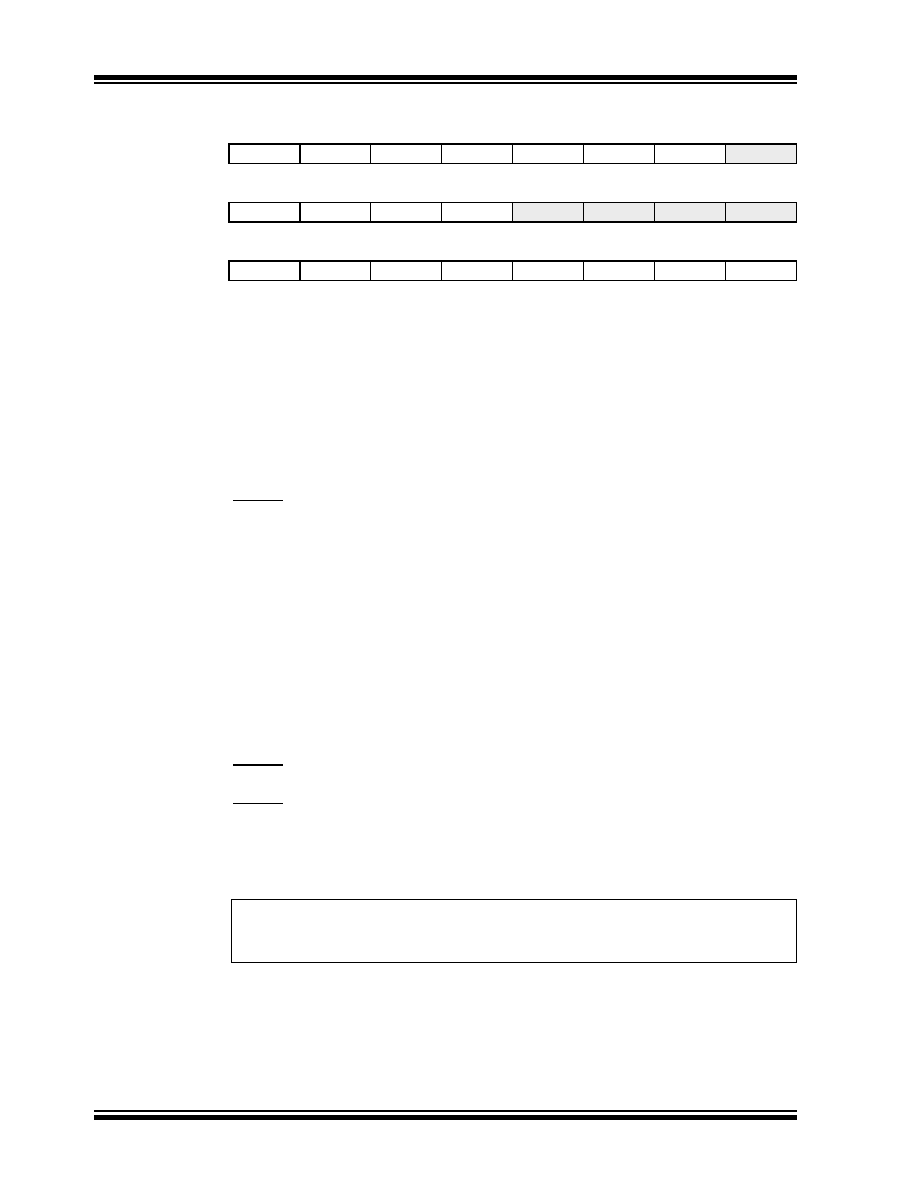
REGISTER 23-1:
CANCON: CAN CONTROL REGISTER
Mode 0
R/W-1
R/W-0
R/S-0
R/W-0
U-0
REQOP2
REQOP1
REQOP0
ABAT
WIN2
WIN1
WIN0
—
Mode 1
R/W-1
R/W-0
R/S-0
U-0
REQOP2
REQOP1
REQOP0
ABAT
—
Mode 2
R/W-1
R/W-0
R/S-0
R-0
REQOP2
REQOP1
REQOP0
ABAT
FP3
FP2
FP1
FP0
bit 7
bit 0
bit 7-5
REQOP2:REQOP0: Request CAN Operation Mode bits
1xx
= Request Configuration mode
011
= Request Listen Only mode
010
= Request Loopback mode
001
= Request Disable mode
000
= Request Normal mode
bit 4
ABAT: Abort All Pending Transmissions bit
1
= Abort all pending transmissions (in all transmit buffers)
0
= Transmissions proceeding as normal
bit 3-1
Mode 0:
WIN2:WIN0: Window Address bits
This selects which of the CAN buffers to switch into the access bank area. This allows access
to the buffer registers from any data memory bank. After a frame has caused an interrupt, the
ICODE2:ICODE0 bits can be copied to the WIN2:WIN0 bits to select the correct buffer. See
Example 23-2 for a code example.
111
= Receive Buffer 0
110
= Receive Buffer 0
101
= Receive Buffer 1
100
= Transmit Buffer 0
011
= Transmit Buffer 1
010
= Transmit Buffer 2
001
= Receive Buffer 0
000
= Receive Buffer 0
bit 0
Unimplemented: Read as ‘0’
bit 3-0
Mode 1:
Unimplemented: Read as ‘0’
Mode 2:
FP3:FP0: FIFO Read Pointer bits
These bits point to the message buffer to be read.
0111:0000
= Message buffer to be read
1111:1000
= Reserved
Legend:
R = Readable bit
W = Writable bit
U = Unimplemented bit, read as ‘0’
- n = Value at POR
‘1’ = Bit is set
‘0’ = Bit is cleared
x = Bit is unknown
发布紧急采购,3分钟左右您将得到回复。
相关PDF资料
XF2J-2424-11
CONN FPC 24POS 0.5MM SMT
PIC18LF6585T-I/PT
IC PIC MCU FLASH 24KX16 64TQFP
PIC18LF6680T-I/PT
IC PIC MCU FLASH 32KX16 64TQFP
XF2J-2224-11
CONN FPC 22POS 0.5MM SMT
PIC18F6525T-I/PT
IC PIC MCU FLASH 24KX16 64TQFP
PIC18F4439-E/ML
IC PIC MCU FLASH 6KX16 44QFN
XF2J-2024-11
CONN FPC 20POS 0.5MM SMT
PIC16LF747-I/ML
IC PIC MCU FLASH 4KX14 44QFN
相关代理商/技术参数
PIC18F85J10-I/PT
功能描述:8位微控制器 -MCU 32 KB FL 2 KB RAM RoHS:否 制造商:Silicon Labs 核心:8051 处理器系列:C8051F39x 数据总线宽度:8 bit 最大时钟频率:50 MHz 程序存储器大小:16 KB 数据 RAM 大小:1 KB 片上 ADC:Yes 工作电源电压:1.8 V to 3.6 V 工作温度范围:- 40 C to + 105 C 封装 / 箱体:QFN-20 安装风格:SMD/SMT
PIC18F85J10-I/PT
制造商:Microchip Technology Inc 功能描述:IC 8BIT MCU PIC18F 40MHZ TQFP-80 制造商:Microchip Technology Inc 功能描述:IC, 8BIT MCU, PIC18F, 40MHZ, TQFP-80
PIC18F85J10T-I/PT
功能描述:8位微控制器 -MCU 32 KB FL 2 KB RAM RoHS:否 制造商:Silicon Labs 核心:8051 处理器系列:C8051F39x 数据总线宽度:8 bit 最大时钟频率:50 MHz 程序存储器大小:16 KB 数据 RAM 大小:1 KB 片上 ADC:Yes 工作电源电压:1.8 V to 3.6 V 工作温度范围:- 40 C to + 105 C 封装 / 箱体:QFN-20 安装风格:SMD/SMT
PIC18F85J11-I/PT
功能描述:8位微控制器 -MCU 32KB Flash 2048BRAM 67I/O RoHS:否 制造商:Silicon Labs 核心:8051 处理器系列:C8051F39x 数据总线宽度:8 bit 最大时钟频率:50 MHz 程序存储器大小:16 KB 数据 RAM 大小:1 KB 片上 ADC:Yes 工作电源电压:1.8 V to 3.6 V 工作温度范围:- 40 C to + 105 C 封装 / 箱体:QFN-20 安装风格:SMD/SMT
PIC18F85J11T-I/PT
功能描述:8位微控制器 -MCU 32KB Flash 2048bytes-RAM 67I/O RoHS:否 制造商:Silicon Labs 核心:8051 处理器系列:C8051F39x 数据总线宽度:8 bit 最大时钟频率:50 MHz 程序存储器大小:16 KB 数据 RAM 大小:1 KB 片上 ADC:Yes 工作电源电压:1.8 V to 3.6 V 工作温度范围:- 40 C to + 105 C 封装 / 箱体:QFN-20 安装风格:SMD/SMT
PIC18F85J15-I/PT
功能描述:8位微控制器 -MCU 48 KB FL 4 KB RAM RoHS:否 制造商:Silicon Labs 核心:8051 处理器系列:C8051F39x 数据总线宽度:8 bit 最大时钟频率:50 MHz 程序存储器大小:16 KB 数据 RAM 大小:1 KB 片上 ADC:Yes 工作电源电压:1.8 V to 3.6 V 工作温度范围:- 40 C to + 105 C 封装 / 箱体:QFN-20 安装风格:SMD/SMT
PIC18F85J15T-I/PT
功能描述:8位微控制器 -MCU 48 KB FL 4 KB RAM RoHS:否 制造商:Silicon Labs 核心:8051 处理器系列:C8051F39x 数据总线宽度:8 bit 最大时钟频率:50 MHz 程序存储器大小:16 KB 数据 RAM 大小:1 KB 片上 ADC:Yes 工作电源电压:1.8 V to 3.6 V 工作温度范围:- 40 C to + 105 C 封装 / 箱体:QFN-20 安装风格:SMD/SMT
PIC18F85J50-I/PT
功能描述:8位微控制器 -MCU 32KB Flash 3936byte RAM RoHS:否 制造商:Silicon Labs 核心:8051 处理器系列:C8051F39x 数据总线宽度:8 bit 最大时钟频率:50 MHz 程序存储器大小:16 KB 数据 RAM 大小:1 KB 片上 ADC:Yes 工作电源电压:1.8 V to 3.6 V 工作温度范围:- 40 C to + 105 C 封装 / 箱体:QFN-20 安装风格:SMD/SMT